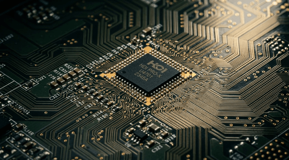
An HDI PCB is a High Density Interconnect printed circuit board that packs far more circuitry into a smaller area than a traditional board. As electronics shrink, standard boards cannot keep up with the demand for miniaturization. These boards solve this with laser-drilled microvias, blind and buried vias, and advanced stack-ups.
This guide explains what an HDI PCB is, how it is made, and how to choose a manufacturer that delivers reliable, high-performance boards. It also covers design considerations and the system-level cost savings that make HDI the standard for modern electronics.
What Is an HDI PCB?
An HDI PCB stands apart because it delivers far higher connection pad density than a standard multi-layer board. It achieves this using microvias, blind vias, buried vias, and advanced stack-up techniques. The result is more routing layers and interconnects in the same or smaller footprint, which is why high density interconnect designs are now standard in modern electronics.
LHD PCB is an experienced manufacturer of high density interconnect boards with more than 20 years in the industry. The company holds UL, ISO, RoHS, and IPC certifications and offers no minimum order quantity with stable quality.
HDI PCB vs Standard PCB
The differences between an HDI PCB and a standard board are substantial. These boards use laser-drilled microvias rather than only mechanical drilling. They rely on blind and buried vias that are rare in standard designs. It achieves far higher wiring density per unit area and better signal integrity with shorter signal paths. Standard boards remain limited by mechanical vias and are generally reserved for commodity and legacy products.
Why Density Matters
Higher density means more functionality in less space. A single board can replace several traditional ones, which reduces assembly time and failure points. This is why compact products such as smartphones, wearables, and medical devices depend on high density interconnect technology.
HDI PCB Process Capabilities
A capable manufacturer must support a broad range of specifications. The key parameters define what a supplier can actually produce.
Layer Count and Structure
Leading manufacturers build boards from 4 to 40 layers and support structures from 1+N+1 through 4+N+4, plus Any-Layer and ELIC designs where nearly every layer interconnects directly. This range is what allows a single HDI PCB to replace several simpler boards.
Fine Features
Advanced production achieves laser microvias as small as 0.075mm, mechanical drills down to 0.15mm, and trace widths of 50 micrometers. These fine features enable dense routing near fine-pitch components.
Materials and Finishes
Common materials include FR4, Rogers, and Panasonic Megtron laminates. Surface finishes range from ENIG and ENEPIG to immersion silver, tin, OSP, and hard gold, giving designers flexibility for different environments.
Special Processes
Backdrilling, cavity boards, and rigid-flex expand what a manufacturer can deliver for complex, high-reliability HDI PCB applications.
Common HDI PCB Stack-Ups
Stack-up structure defines how a board routes signals through its layers. Each type suits a different level of complexity.
1+N+1 Stack-Ups
Basic HDI PCB Stack-Ups
The simplest HDI structure, ideal for small form-factor electronics where cost efficiency matters most.
2+N+2 Stack-Ups
Mid-Complexity HDI PCB Stack-Ups
Common in smartphones and mid-complexity boards, balancing density with manufacturability.
3+N+3 and Any-Layer Designs
Used in telecom, 5G, AI, and complex consumer boards where maximum interconnect density is required.
Rigid and Rigid-Flex HDI
Chosen for wearables, medical devices, and aerospace, where boards must flex or fit unusual enclosures.
The HDI PCB Manufacturing Process
Manufacturing these boards involves a series of tightly controlled steps that determine long-term reliability.
Inner Layer Preparation
Starting the HDI PCB Build
Copper foil is applied to the core laminate, then patterned through imaging and etching. Clean edge definition and strong copper adhesion improve yield.
Sequential Lamination
Advanced HDI uses multiple lamination passes, adding layers one at a time. This creates the buried and blind vias that define high density interconnect designs.
Laser Drilling
Microvias are cut with a laser, often less than 100 micrometers in diameter. Laser drilling is essential to the interconnect density these designs provide.
Copper Plating and Via Filling
Resin-filled microvias are plated with copper for conductivity. Via-in-pad structures receive special planarization for smooth component mounting.
Inspection and Testing
Automated optical inspection, X-ray analysis, electrical testing, and reliability testing confirm that each board meets its specification.
HDI PCB Design Considerations
Good design separates a cost-effective board from a flawed one. Engineers focus on several key areas.
Plan the Stack-Up Early
Designing an HDI PCB for Manufacturability
Model the sequential build and via placement during design. Early EMI modeling, impedance calculation, and thermal simulation prevent costly late revisions.
Keep Microvia Aspect Ratios Low
Use aspect ratios of 1:1 or less for laser-drilled microvias. This maximizes quality and long-term reliability.
Place High-Pin Components First
Identify BGA, HDMI, USB, and RF parts early, then route HDI features directly beneath them for optimal density.
Balance Cost and Complexity
Not every board needs the highest HDI level. Match the HDI structure to the actual performance and space requirements.
System-Level Cost Savings
These boards may cost more per unit than a standard PCB, but the system-level economics favor high density interconnect.
Fewer Boards Required
Higher wiring density means one board can replace multiple standard boards, cutting assembly, inspection, and handling costs.
Smaller, Lighter Products
More functions on a single board produce smaller devices and less expensive enclosures, a key advantage in smartphones and satellites.
Lower Assembly and Test Costs
Fewer boards and components mean faster assembly, lower logistics costs, and fewer failure points across the product.
Faster Time to Market
Fewer layers and streamlined assembly help new products reach the market faster, which matters in competitive consumer electronics.
Real-Time Market Context
The market continues to expand with the growth of compact electronics. Industry research from The Business Research Company values the global high density interconnect market at about $19.47 billion in 2026, projected to reach $28.82 billion by 2030 at a 10.3% compound annual growth rate. Other estimates place the broader market even higher, around $21.6 billion in 2026.
Growth is driven by 5G networks, electric vehicle electronics, AI and high-performance computing, and the ongoing miniaturization of consumer devices. Asia-Pacific remains the largest and fastest-growing region, reflecting its deep electronics manufacturing base. This demand is why reliable high density interconnect manufacturing has become a strategic priority for electronics companies worldwide.
How to Choose an HDI PCB Manufacturer
The precision required for HDI means manufacturer selection matters greatly.
Verify HDI Expertise
Choosing an Experienced HDI PCB Partner
Confirm proven experience with microvias, blind and buried vias, and advanced stack-ups. Ask for examples of similar projects.
Check Technology and Inspection
The manufacturer should offer in-house laser drilling, AOI, microsection analysis, and X-ray inspection with certified sequential lamination.
Look for Design Support
Choose a partner who reviews your design, suggests layer reductions, and helps with EMI modeling during the design phase.
Confirm Certification and Flexibility
IPC, ISO, and IATF certifications matter for high-reliability fields. Fast prototyping and scalable volume manufacturing support your time-to-market goals.
Frequently Asked Questions
What is an HDI PCB?
An HDI PCB is a High Density Interconnect printed circuit board that uses microvias, blind vias, and advanced stack-ups to pack more circuitry into a smaller area.
What is the difference between HDI PCB and standard PCB?
An HDI PCB uses laser-drilled microvias and blind or buried vias for far higher wiring density, while standard boards rely on mechanical vias and offer lower density.
What are microvias in an HDI PCB?
Microvias are tiny laser-drilled holes, often under 100 micrometers, that connect adjacent layers and enable the dense routing of an HDI PCB.
How many layers can an HDI PCB have?
Leading manufacturers produce HDI PCBs from 4 layers up to 40 layers or more, supporting structures from 1+N+1 through Any-Layer and ELIC designs.
Why is an HDI PCB more cost-effective overall?
Although the bare board costs more, higher density means fewer boards, less assembly, and smaller products, lowering the total system cost.
What industries use HDI PCBs?
HDI PCBs serve smartphones, medical devices, automotive electronics, telecom and 5G, AI computing, wearables, and aerospace systems.
Conclusion
An HDI PCB is the backbone of modern miniaturized electronics, delivering the density, signal integrity, and reliability that standard boards cannot match. Through laser-drilled microvias, sequential lamination, and careful stack-up design, manufacturers pack more performance into smaller spaces while lowering total system cost. As the high density interconnect market grows toward $29 billion by 2030 on the strength of 5G, electric vehicles, and AI, choosing the right HDI PCB partner becomes a competitive decision. Select a manufacturer with proven HDI expertise, in-house inspection, and design support, and your products will meet the demands of the next generation of technology.